University of Missouri-University of the Western Cape Academic Exchange Program
Report
Candidate: Prof Christopher Arendse, Department of Physics and Astronomy, University of the Western Cape (UWC)
Host: Prof Suchi Guha, Department of Physics and Astronomy, University of Missouri-Columbia (UMC)
Period: January 17 – February 16, 2019
-
Objectives of the visit
The specific objectives for the initial phase of this collaborative project, entitled
Chemical vapor deposition of perovskite thin films for functional devices, were:
- To design and construct a chemical vapor deposition (CVD) at UMC for the deposition of perovskite materials
- To demonstrate the deposition of a MAPbI3 perovskite thin film at a high deposition rate, improved uniformity and crystallinity
- To incorporate the optimized perovskite layer into a functional device
- To identify possible synergies between the Department of Physics and Astronomy at UWC and its counterpart at UMC and to explore student exchanges.
-
Milestones Achieved
Design and construction of CVD reactor:
A thermal chemical vapor deposition (CVD) system was designed and constructed in Prof Guha’s laboratory that can be used to deposit a variety of thin films and nanostructures, by either vapor or chemical vapor deposition. The design of the system is based on a similar system at UWC.
The reactor is composed of a horizontal quartz-tube, enclosed by a 3-zone split-tube furnace, where each zone can be independently heated to 1200 °C using specialized temperature controllers. The base pressure in the system amounts to 10-1 bar, which is achieved with a rotary vane pump. The system also has a nitrogen gas supply, where the flow rate is controlled by a mass flow meter, with an exhaust through a bubbling system. Figure 1 (below) show a schematic of the CVD reactor. It should be noted that the setup of the system had some technical challenges, which was speedily addressed by the workshop personnel in the department. Due to the afore-mentioned technical support, the system design, setup, and testing was completed after week 1.
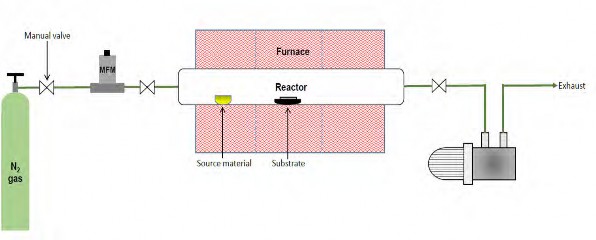
Fig. 1: Schematic of the CVD reactor at UMC
Deposition of perovskite thin films:
Methyl-ammonium lead iodide (MAPbI3) perovskite films were successfully deposited using the above-mentioned system by a 2-step process. For the deposition of the lead iodide (PbI2) thin films (Step 1), lead (II) iodide powder in a ceramic boat was placed in the centre of the first zone and glass substrates were placed downstream at various distances away from PbI2 source, all mounted on a ceramic substrate holder. The first zone was subsequently ramped at 10 °C/min up to a nominal temperature of 400 °C, which is above the known sublimation temperature of PbI2. Nitrogen gas (N2) at a specific flow rate was used to transport the PbI2 vapours towards the substrates. The deposition time amounted to 40 minutes. Thereafter, the N2 flow was interrupted and the samples were allowed to cool to room temperature. A yellowish, compact PbI2 thin film was produced and no post treatment was performed on the PbI2 thin films. The purpose of this study was to investigate the effect of the substrate distance from the source (dss) on the thickness, morphology, optical properties and crystal structure of the resultant PbI2 thin films. Optical microscopy and scanning electron microscopy confirm a dense, homogeneous thin film with superior grain sizes in excess of 2 µm. UV/VIS measurements confirm a pure PbI2 thin film with characteristic peaks present and a thickness dependence on dss, with values between 80 and 190 nm.
The perovskite conversion of the PbI2 thin films (Step 2) was performed in the afore-mentioned CVD system. Methyl ammonium iodide (MAI) salt was placed in a fresh ceramic boat at the optimized distance from PbI2 thin films. The temperature of the MAI boat was subsequently ramped at 10 °C/min up to a nominal temperature of 200 °C. The MAI vapours were transported towards the PbI2 thin films by a N2 flow. The conversion time amounted to 90 minutes, after which the samples were allowed to cool to room temperature in the reactor with N2 flow. A clear colour change was observed in the thin films from yellow to dark-brown or black (depending on the PbI2 thickness). UV/VIS measurements confirm the perovskite conversion with bang gap around 1.55 eV. Furthermore, no PbI2 peaks were observed, which confirms full conversion. It must also be noted that these samples retained their dark colour in ambient conditions, which speaks to its improved stability, as opposed to solution-processed perovskites that change back to PbI2 after exposure to air. It is expected that these perovskite thin films are of superior quality, as its grain size will be in excess of 2 µm. Scanning electron microscopy and x-ray diffraction measurements are required to confirm this.
Device manufacturing:
The optimized perovskite thin film was deposited on ITO-coated glass and n++-doped Si/SiO2 substrates for incorporation into thin film transistor devices (two device architectures). In addition, the substrates were sent to UWC for similar depositions using the CVD reactor there. The device characterization was performed at UMC, with poor performance, which we suspect are due to the environmental factors. These devices will be repeated and the device performance will be measurements in vacuum.
Sample characterisation – UWC samples:
Polymer, perovskite, titanium dioxide and zinc oxide samples from UWC were characterized at UMC by techniques unavailable at UWC. These include micro-Raman spectroscopy and vacuum photoluminescence. The results were further analysed at UMC and forms part of MSc and PhD projects of students based at UWC.
Student involvement:
I was privileged to work with talented post-doctoral and PhD students of Prof Guha on the CVD growth of perovskites. Of specific mention is the interesting discussions on the high-pressure exposure of the perovskites. In addition, two PhD students from UWC are currently involved in this project with topics related to the organic-inorganic and all-inorganic perovskites for solar cell and TFT application, respectively.
Interactions and Synergies:
During my visit, I met with the following UM faculty:
-
Prof Paul Miceli, my collaborator on the silicon-nanowire project where we supervise one PhD student. We have explored new projects and reviewed a manuscript that is due for submission for publication (PhD student).
-
I was invited to be part of a discussion/presentation on high-pressure exposure of inorganic perovskites, hosted by Prof Suchi Guha and her post-doc, Dr. Sorb Yesudhas. Other participants included Prof Yangchuan Xing and Ms. Mariia Goriacheva from the Chemistry department at UMC.
-
I was also invited to the PhD thesis defense of Dr Amrit Laudari (supervisor – Prof Guha), with thesis entitled: "Polarization-induced transport in organic field-effect transistors".
-
Prof Suchi Guha, Prof Paul Miceli, Prof Angela Spec and I met with Prof Nicole Monnier, Associate Dean for Undergraduate Studies, to explore student exchanges between UWC and UMC. It was evident that reciprocal post-graduate exchanges would be valuable in the Astrophysics and Condensed Matter Physics fields. Funding possibilities will be explored.
-
Prof Paul Miceli and I also had a lunch meeting with the Interim Vice Provost for International Programs at the University of Missouri, Prof Mary Stegmaier.
-
I also met with Prof Guang Blan to discuss envisaged collaborations with the Astrophysics group at UWC.
-
Finally, I met with Prof William Fahrenholtz from Materials Science and Engineering, Missouri University of Science and Technology to explore possible synergies between our departments.
Presentation:
On January 31, 2019, I presented a 1-hour seminar entitled: “Hybrid perovskite thin films by sequential low-pressure vapor deposition in a single reactor” to an audience composed of mainly Condensed Matter Physicists. The main goal of the presentation was to communicate the versatility of chemical vapor deposition and the resultant stable thin films that it produces. The presentation was well received and provoked some interesting discussions afterwards.
-
-
Value of the UM / UWC Exchange Program
The exchange program allowed for an active cooperation between the groups at UWC (with expertise in CVD and structural properties) and UMC (with expertise in device manufacturing and opto-electronic properties). The UMC group now have capability to produce thin films and nanostructures on-site. The UWC group has gained insight into the device manufacturing and performance monitoring systems required, for which funding will be sourced to setup similar facilitates at UWC. This synergy will aid in the investigation into the relationship between the chemical and morphological structures of perovskite materials, the processing conditions of the device, and their optoelectronic properties. Through this exchange, I also gained access to state-of-the-art equipment and expertise and engaged with world-renowned researchers with expertise ranging from Condensed Matter Physics and Astronomy to Physics Education. As in my case, this program will have a definite positive impact on the intellectual development and career advancement of both young and established researchers.
-
Challenges and Suggestions
The planning and preparation of this visit was perfect and for that, I commend the International Relations Office of UWC and the Office of the President of UM.
-
Acknowledgements
I acknowledge the financial support of the UM / UWC Exchange Program and the support of Prof Rod Uphoff, Ms. Hilda Wilson and their teams for the planning and arrangements. The National Research Foundation is also acknowledged for co-funding this exchange visit. I wish to thank Prof Suchi Guha and the Department of Physics and Astronomy at UMC for hosting me. I especially express my gratitude to Prof Suchi Guha, Prof Carsten Ullrich, Prof Paul Miceli and his wife, Marta, for their friendship, hospitality and support and for the great dinners, discussions and excursions. I also wish to thank Prof Peter Pfeifer for initiating our departmental collaboration with UMC and for his friendship, valuable discussions and advice. A special thank you to the team of Prof Guha (Sorb, Amrit, Alec and Randy) for the valuable discussions and for their assistance with the analytical measurements!
Reviewed 2025-12-23